The interconnect subsystem is called "Data Fabric", which knows so called coherent slaves according to the last enumeration list.
There is a new L0 ITLB, which is the only level 0 thing being mentioned so far, while VR World mentioned level 0 caches (besides other somewhat strange rumoured facts like no L3 cache in the APU variant - while this has been shown on the leaked Fudzilla slide). The only thing resembling such a L0 cache is a uOp cache, which has clearly been named in the new patch in a section related to the decode/dispatch block (indicated by "de"):
There are strings for both a "uop cache" and a "uop buffer". So far I knew about this uop buffer patent filed by AMD in 2012, which describes different related techniques aimed at saving power, e.g. when executing loops or to keep the buffer physically small by leaving immediate and displacement data of decoded instructions in an instruction byte buffer ("Insn buffer") sitting between instruction fetch and decode. The "uop cache" clearly seems to be a separate unit. Even without knowing how many uops per cycle can be provided by that cache, it will help to save power and remove an occaisional fetch/decode bottleneck when running two threads. The next interesting block is about the execution units:
Here is a first confirmation of a checkpoint mechanism. This has been described in several patents and might also be an enabler for hardware transactional memory, which has been proposed in the form of ASF back in 2009. Another use case is the quick recovery from branch mispredictions, where program flow can be redirected to a checkpoint created right before evaluating a difficult to predict branch condition.
There is a confirmation of the "GMI link".
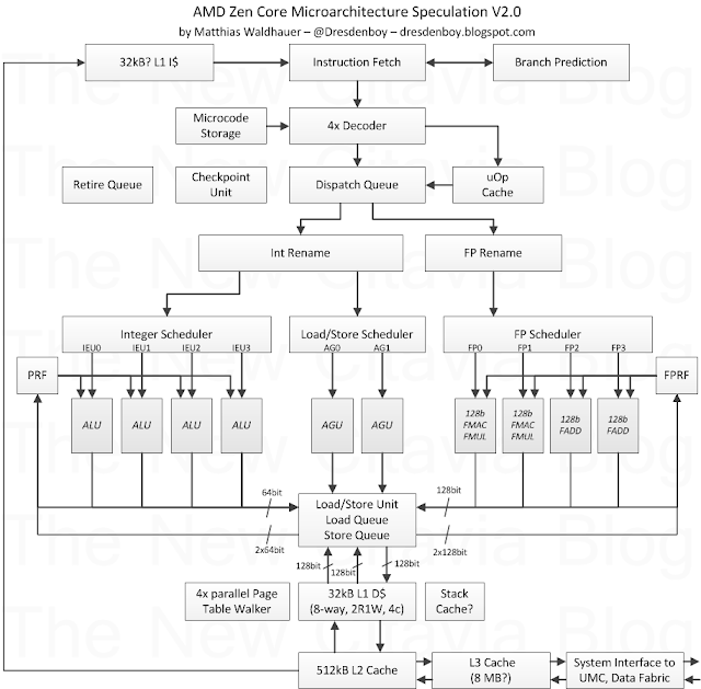
Notable changes are:
uOp Cache has been added based on the new patch
FMUL/FADD for FMAC pairing removed, based on some corrections of the znver1 pipeline description.
4x parallel Page Table Walkers added, based on US20150121046
128b FP datapaths (also to/from the L1 D$) based on "direct" decode for 128b wide SIMD and "double" decode for 256b AVX/AVX2 instructions
32kB L1 I$ has been mentioned in some patents. With enough ways, a fast L2$ and a uOp cache this should be enough, I think.
issue port descriptions and more data paths added
2R1W and 4 cycle load-to-use-latency added for the L1 D$ based on info found on a LinkedIn profile and the given cylce differences in the znver1 pipeline description
Stack Cache speculatively added based on patents and some interesting papers. This doesn't help so much with performance, but a lot with power efficiency